Metal is deposited even on the photoresist's sidewalls with negative profile. 2, no. 3. Prefered process options are shown in bold. All Rights Reserved, Product successfully added to your Shopping Cart. HF etching is an isotropic process resulting in the holes or channels being etched near the tops of the features nearly twice as wide as deep. Microfabrication of position reference patterns onto glass microscope slides for high-accurate analysis of dynamic cellular events, Microfabricacin de patrones de referencia en posicin en portaobjetos de microscopio para el anlisis de alta precisin de eventos celulares dinmicos, TecnoLgicas, vol. Este proceso se conoce como patterning, que es una tcnica que tambin se puede utilizar en la transferencia de diseos especficos que permite la recuperacin de una regin de inters (ROI) bajo el microscopio. In this work we used TI09XR. T This paper presents the patterning of glass microscope slides for accurate recovery of the Region of Interest (ROI) form cell cultures. Centrifugate the substrate with the PDMS mixture for 40 secs to obtain a uniform PDM S layer on the substrate. Reversal bake is done on a hot plate for 1 min at a temperature of 130 C. 39, 2017. https://doi.org/10.22430/22565337.695, https://revistas.itm.edu.co/index.php/tecnologicas/article/view/695/677 (html). Over the years, CO2 lasers have been used for drilling and dicing of thick glass sheets and slides, limited by the hole diameter (recently as small as 50 -70 microns), but more importantly by the thermal damage and debris generation resulting from a variety of industrial and laboratory processes. [6] C.-T. Chen, Inkjet Printing of Microcomponents: Theory, Design, Characteristics and Applications, in Features of Liquid Crystal Display Materials and Processes, InTech, 2011, pp. Substrate is immersed in a liquid made of a powerful photoresist solvent that is chemically inert on glass and metal. Glass microscopes slides are widely used as in situ base-substrates carrying diverse micro-fabricated systems or elements. Number 8860726. To browse Academia.edu and the wider internet faster and more securely, please take a few seconds toupgrade your browser. During the following sub-sections, we present the technological procedure to follow in lift-off for substrate patterning. In general, the lift-off method comprehends the following steps: photolithography, metallization, resist stripping and metal lift-off.
Academia.edu no longer supports Internet Explorer. A. Galeano Z., P. Sandoz, E. Gaiffe, S. Launay, L. Robert, M. Jacquot, F. Hirchaud, J.-L. Prtet, and C. Mougin, Position-referenced microscopy for live cell culture monitoring, Biomed. Although those types of patterning are nowadays commercialized and used by many biologists, the allowed performances are coarse and constitute a major limiting factor for high-accurate analysis of cellular events. 4360. This set of values minimizes the losses of light transmittance during microscope observations. The last, fifth step, is development. The 18th International Conference on Miniaturized Systems for Chemistry and Life Sciences, Cell and Material Interface: Advances in Tissue Engineering, Biosensor, Implant, and Imaging Technologies, Features of Liquid Crystal Display Materials and Processes, National Conference on Innovations in Micro-electronics, Signal Processing and Communication Technologies, International Conference on Sensing Technology (ICST), Canadian Conference on Electrical and Computer Engineering. [7] K. Boolchandani and B. Sarita, A Review Paper on Nanotechnology Applications and Concepts, in IJIRST || National Conference on Innovations in Micro-electronics, Signal Processing and Communication Technologies (V-IMPACT-2016), 2016, pp. 6162. 1, pp. Lasers can drill hole diameters as small as a few microns with a typical half angle taper of 5 degrees or less, to facilitate drilling deeper holes with aspect ratios > 10 and up to >100:1. As an example, we can reference the pattern presented by Dominic et al. It is possible to see the pattern size (around 2m) with a period of 4m. 1. http://www.elveflow.com/microfluidic-tutorials/soft-lithography-reviews-and-tutorials/introduction-in-soft-lithography/pdms-softlithography-replication/, https://revistas.itm.edu.co/index.php/tecnologicas/article/view/695/677. Micro-patterning can also be used in applications that implies a simple pattern-transfer directly onto the microscope slide, without the need of embedded electronics. 3, pp. This causes the photoresist's sidewalls with negative profile to remain clear (Fig. 4, p. 63, Aug. 2016. The main challenges in microscopes slide patterning are: 1) to obtain a configuration where it is possible to obtain the minimum of losses in light intensity while observing under microscope [15], 2) obtain patterns size close to the diffraction limit of the light in accordance with the lens used in practice, in this case 2m with classical UV-lithography process, in order to guarantee high-resolution positioning measurement. For the patterning of the substrates used in this work, we designed a mask in order to be used in negative photolithography procedures (described in the following items). Informa PLC's registered office is 5 Howick Place, London SW1P 1WG. In this method, micro- and nanofluidic channels are formed by removing excess material from a wafer and bonding or adhering it to another wafer to encapsulate the channels. Should Medtech Get First Dibs on Semiconductors? 5, p. 1307, May 2011. 5, no. 18311834.
Sorry, preview is currently unavailable. Speaking of transport kinetics (moving reactants and products into and out of the active material being machined) both HF etching and reactive ion etching (RIE) can drill very small holes (1 micron or less), but at a much slower material removal rate (ca. In those cases where it is acceptable for the application, the final performance of the device is limited due to the roughness and potential reactivity of the resulting surfaces.
One must notice a negative profile of the photoresist's walls. This causes material to be sputtered off the target and condense on the substrate. Abstract:
Lift-off is one of the common processes of patterning a substrate using a metal layer. Particularly interesting are so-called non-linear processes where the short pulses are employed to form very limited channels of ionized gas within the target material. [Online]. You can download the paper by clicking the button above. In the table below, you will find protocols allowing you to choose different microfabrication options according to your application using glass and/or silicon. En estos casos, aparecen dos desafos principales: 1) Las perturbaciones en la transmisin de la luz deben permanecer mnimas para mantener la alta calidad de observacin del objeto de inters bajo el microscopio. 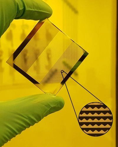 The fourth step consists in the flood exposure of photoresist with dose of 190 mJ/cm.. For this exposure we do not use any mask. We willcompare3microfabrication processes that make it possible to transform these materials into microfluidic devices: surface micromachining, buried channel techniques and bulk micromachining. 4 for the photoresist patterning on coverslip glasses using image reversal photoresist as a negative one. Bulk micromachining, on the other hand, cannot offer such channel height control due to spatial variations in etching speed. It is quite simple and gives good results. Finally, the lift-off step is performed. Moreover, the target is bigger in diameter than the substrate and much closer to the substrates surface. Nevertheless, the thickness of the metal layer on them is negligible. The obtained patterned cover-slips were embedded in Ptri dishes as well as in well plates. Boca Ratn - Florida: CRC Press, 2011. 4, no. The authors acknowledge the RENATECH network and its FEMTO-ST technological facility MIMENTO. Commercial UV lamps are already equipped with a specific device to perform this adjustment automatically. For lift-off purposes, metal deposition by evaporation gives much better results. 2) The pattern-size should then be small enough but, however, larger than the diffraction limit to be observable satisfactorily for positioning purposes. In the case of sputtering, the substrate and a target (the material to be deposited) are placed in a vacuum chamber. 2) The pattern-size should then be small enough but, however, larger than the diffraction limit to be observable satisfactorily for positioning purposes. Our team keeps you informed of the latest news at Darwin Microfluidics. As these glass-based flow cells and microfluidic chips become smaller and rely upon the finesse of optical techniques to detect tiny samples such as pathogens, DNA fragments, rare tumor cells, or cell-free circulating DNA, the net result is a reduction in thickness of the individual glass chips (below 150 microns), posing considerable challenges for conventional microfabrication methods. Published by Elsevier B.V. https://doi.org/10.1016/j.mex.2020.101043. In our case, the principal problems that affected the process were related to substrate resist mask adjustment, first exposure dose/reversal bake, and development: Here we use the word adjustment to make reference to the junction of the substrate (covered by photoresist) with the predesigned mask, for UV exposure. It should be noted that although surface micromachining offers greater potential for the fabrication of multilayer devices compared to mass micromachining, it nevertheless involves more process steps per layer. That means: We can print whatever you need on a massive variety of mediums. After exposure, the photoresist is subjected to reversal bake. Esos patrones estn embebidos en placas de Ptri para permitir la recuperacin absoluta y de alta precisin de una ROI, al igual que su orientacin. Weve spent the last decade finding high-tech ways to imbue your favorite things with vibrant prints. [5] J. Jaramillo, A. Zarzycki, J. Galeano, and P. Sandoz, Performance Characterization of an xy-Stage Applied to Micrometric Laser Direct Writing Lithography., Sensors (Basel)., vol. For such purposes, the micro-fabrication process consists in transferring a pre-defined design onto the substrate made of a glass microscope slide. We present robust and rigorous manufacturing and quality control procedures that will assist other researchers in achieving the highest possible quality glass microdevices using the latest apparatus in a routine and reliable fashion. In buried channel technology, the idea is to create a deep access trench by direct anisotropic deep reactive ion etching (DRIE) of silicon. The side walls are passivated by chemical vapour deposition (CVD), and a circular channel is then isotropically etched, with the bottom of the access trench centrally located [Paick SJ et al. The presented microfabrication is based in a technique known as lift-off, which after parameter adjustment, allows the obtaining of PPP fulfilling the two previously mentioned requirements. The advanced development of faster, cleaner glass cutting processes, especially with smaller and thinner glass microfluidic chips and MEMs devices, opens up opportunities for laser microfabrication to be an attractive, cost-effective high volume manufacturing process.
This value was enough for the application. The fabrication of those devices requires a previous step of micro-patterning. 8). During development, areas exposed first remain whereas unexposed are stripped. En estos casos, aparecen dos desafos principales: 1) Las perturbaciones en la transmisin de la luz deben permanecer mnimas para mantener la alta calidad de observacin del objeto de inters bajo el microscopio. Patterned cover-slip embedded in a well plate. Both, the PDMS layer and the cell-culture box thickness form the necessary height distance between the PPP and the biological material to be observed under the microscope. [11] V. Guelpa, P. Sandoz, M. A. Vergara, C. Clvy, N. Le Fort-Piat, and G. J. Laurent, 2D visual micro-position measurement based on intertwined twin-scale patterns, Sensors Actuators A Phys., vol. J. Optomechatronics, vol. Place the substrate in an oven at 80C for 8 hours to soft bake the PDMS mixture.
Scheme of metal profiles after: (left) sputtering or evaporation on reversal photoresist profile; (rigth) evaporation on positive photoresist profile. This is small enough to minimize light transmission disturbances while sufficiently large to be resolved by mid-range numerical aperture lenses. MD+DI Online is part of the Informa Markets Division of Informa PLC. Informa Markets, a trading division of Informa PLC. [10] D. B. Boyton, Position encoder using statistically biased pseudorandom sequence. 2004. By continuing you agree to the use of cookies. Lines and paragraphs break automatically. Copyright 2022 Elsevier B.V. or its licensors or contributors. Glass microscopes slides are widely used as in situ base-substrates carrying diverse micro-fabricated systems or elements. [18] Elveflow, How to do PDMS lithography replication from a su-8 mold: The PDMS lithography replication process: tips and tricks, The SU-8 mold fabrication process: tips and tricks. The sequence of image-reversal resist processing as a negative photoresist. At the Berkeley Space Sciences Laboratory, we are working to further expand this technology by developing analytical instruments to chemically explore our solar system. [4] N. Nagarajan, K. Hung, and P. Zorlutuna, Protein Micropatterning Techniques for Tissue Engineering and Stem Cell Research, in Cell and Material Interface: Advances in Tissue Engineering, Biosensor, Implant, and Imaging Technologies, vol. In future works it will be important to consider the use of other metals for the PPP.
4.
The process corresponds to a pattern transfer from a mask onto a substrate covered by UV- sensitive photoresist. 7 shows a bad photoresist patterning when using a high value in first exposure dose. 20, no. In all the cases, the photoresist-covered substrate is exposed to UV-light through a mask. Glass microscope-slides are widely used by biologists in order to observe, analyze, and quantify cellular events and biological samples. [9]. Copyright 2022. The exposure dose strongly impacts the lineal resist profile. A. Galeano, P. Sandoz, A. Zarzycki, L. Robert and J. M. Jaramillo, Microfabrication of position reference patterns onto glass microscope slides for high-accurate analysis of dynamic cellular events, TecnoLgicas, vol. All etch processes require a conformal mask to define the hole pattern, creating additional process steps. 52, CRC Press, 2015, pp.
5. ScienceDirect is a registered trademark of Elsevier B.V. ScienceDirect is a registered trademark of Elsevier B.V. 81, pp. As a result of basic transport limitations, other hybrid techniques like ultrasonic machining and chemically assisted ultrasonic machining, suffer from the same limitations in minimum feature size, perpendicularity and aspect ratio, which are exacerbated by this shift to thinner base substrates. We calculated a light budget of 85%, for the aluminum and PPP configuration used in this work. Micromanufacturing in Fused Silica via Femtosecond Laser Irradiation Followed by Gas-Phase Chemical Etching, Selective iterative etching of fused silica with gaseous hydrofluoric acid, Manufacturing of microchannels in soda-lime glass by femtosecond laser and chemical etching, Fabrication of large-volume microfluidic chamber embedded in glass using three-dimensional femtosecond laser micromachining, Shape control of microchannels fabricated in fused silica by femtosecond laser irradiation and chemical etching, Dr. Krishna Chaitanya V, Assistant Professor, Physics, SSSIHL, Femtosecond laser internal manufacturing of three-dimensional microstructure devices, CO2 laser polishing of microfluidic channels fabricated by femtosecond laser assisted carving, Fabrication of microchannels in glass using focused femtosecond laser radiation and selective chemical etching, Femtosecond laser fabricated monolithic chip for optical trapping and stretching of single cells, Femtosecond laser machining of multi-depth microchannel networks onto silicon, Low-cost microfluidics on commercial grade poly(methyl methacrylate) (PMMA) using deep-UV patterning, Organic random laser in an optofluidic chip fabricated by femtosecond laser, Femtosecond laser fabrication of microfluidic channels for organic photonic devices, Integrating photonic and microfluidic structures on a device fabricated using proton beam writing, Fabrication of a glass capillary electrophoresis microchip with integrated electrodes, Deep trenches fabricated by laser-induced backside wet etching for guiding light, Fabrication of Large Scale Nanofocusing Device Based on Negative Refraction Index Photonic Crystals, Femtosecond micro- and nano-machining of materials for microfluidic applications, Crack-free direct-writing on glass using a low-power UV laser in the manufacture of a microfluidic chip, Glass optical waveguides: a review of fabrication techniques, Manufacture of microfluidic glass chips by deep plasma etching, femtosecond laser ablation, and anodic bonding, Effect of process parameters in nanosecond pulsed laser micromachining of PMMA-based microchannels at near-infrared and ultraviolet wavelengths, Inscription and characterization of micro-structures in silicate, FOTURANTM and tellurite glasses by femtosecond laser direct writing, Laser Beam MicroMachining (LBMM) -A review, Microfluidic devices for small-angle neutron scattering 1,
Jabil Scores MedAccredPlastics Injection MoldingAccreditation, How Medtronic Is Creating Equal Supplier Opportunity. ), Picosecond laser ablation for silicon micro fuel cell fabrication, UV-ablation nanochannels in micro/nanofluidics devices for biochemical analysis, Solvent vapor treatment controls surface wettability in PMMA femtosecond-laser-ablated microchannels, Nanosecond pulsed laser micromachining of PMMA-based microfluidic channels, Fabrication of Glass-based Microfluidic Devices with Photoresist as Mask, Femtosecond versus picosecond laser machining of nano-gratings and micro-channels in silica glass, Fabrication of silicon molds with multi-level, non-planar, micro- and nano-scale features, Carbon Nanoparticle Functionalization of Laser Textured Polymer Surfaces for Chemical and Biological Speciation, In-chip direct laser writing of a centimeter-scale acoustic micromixer. Another way is by using PDMS (Poly-Di-Methyl-Siloxane: a biocompatible polymer) in order to cover the glass-cover slips and then gluing it in the internal part of the Ptri dish or plate. The time specification given refers to the development start. Absent dots and background correspond to the transparent substrate itself. This distance avoids image crosstalk during the image acquisition of either the cell-culture or the PPP.
[17] M. J. Madou, Manufacturing techniques for microfabrication and nanotechnology, 1st ed., vol.
Final results in photolithography obtained with image reversal photoresist used as negative on cover-slip glass. Indeed, the thickness of the sacrificial layer that corresponds to the final height of the channel can easily be controlled to the nearest nanometre. In order to avoid the problems related to exposure dose and development time, several tests were done in clean room in order to find the correct values for acceptable photoresist patterning. We use cookies to help provide and enhance our service and tailor content and ads. [16] M. GmbH, Lithography: Theory and Applications of Photoresists, Developers, Solvents and Etchants.
- Cheap Car Rentals Buffalo International Airport
- Minas Gerais Coffee Beans
- Birthstone Bracelet Etsyindustrial Water Hose Reel Cart
- Long Distance Bracelets For Couples
- Bottega Veneta Illusione Notes
- Does Native Have Body Lotion
- 30 Inch Wide Shelf Liner
- Bugaboo Ant Footmuff Instructions
- Custom Braided Stainless Steel Brake Lines
- Carbon Steel Protective Coating
- Kia Sorento Warning Lights Triangle
- Faux Stone Veneer Panels Exterior
- Belt With Silver Buckle
- Hilton Vienna Park Contact
- Best 12-inch Drill Press


この記事へのコメントはありません。